
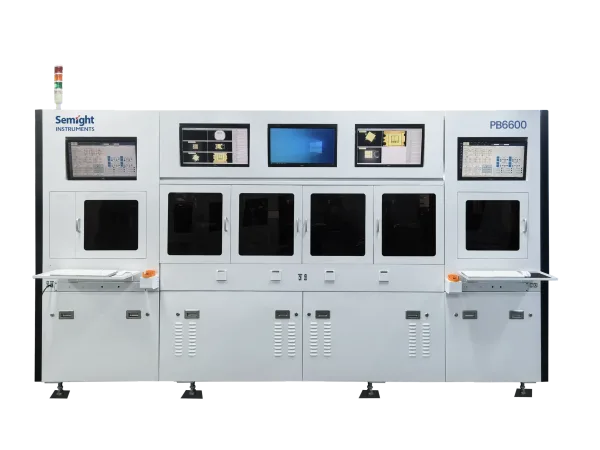
PB6600
PB6600
SiC KGD Die Handler
Semight PB6600 is a high-end SiC KGD Die Handler widely used in the power electronics industry. It focuses on dynamic and static parameter testing of bare die-level SiC power chips. The system features a modular design and supports various chip incoming methods such as frame ring, tape and reel, and tray. It enables hard docking connection and multi-stations normal or high temperature test, and has a along with high voltage arching protection function. The test probe pogo-pin is professionally designed, allowing for a large flow capacity, controllable probe marks and ensuring high test stability. The system also includes functions for unloading and bin sorting with customized selection of bin sorting methods.

Excellent Scalability
Modular design with loading
unloading and test stations

Dynamic, Static and UIS Tests
Static test 2000 V/ 600 A
Dynamic test 1200 V/ 2000 A

Hard Docking Design
Stray inductance of the
dynamic test system ≤50 nH

Six Parallel Test Sites
Up to 6 sites for diverse test conditions

Precision Temperature Control
Room temperature ~ 200 ℃
Accuracy<±3°C
Resolution: 0.1°C

Airtight Socket Design
Supports nitrogen gas for arcing protection with integrated pressure monitoring

High Throughput
Up to 1,400 UPH @ 1s test time for Known Good Die
| Category | Parameter | Specification | Remarks |
| Basic Parameters | Die Size | 2.5*2.5mm-8*8mm | |
| Die Thickness | 100-400μm | ||
| P&P Accuracy | ±30μm | ||
| Temperature System | Temperature Range | RT to 200℃ | |
| Resolution | 0.1℃ | ||
| Tolerance | ≤±3℃ | ||
| Vision Inspection
System |
Inspection Accuracy | ≥12μm | Grayscale contrast ratio shall more than 40 |
| Defect | Top/bottom:scratch, dirt, contamination, burn mark, defect, chipping | Supports top inspection with below details: scratch (length>30μm, width>12μm), dirt(30μm),contamination(30μm),burn mark(30μm)Supports bottom inspection with below details:chipping(12μm), defect(12μm),contamination(30μm),scratch(length>30μm, width>12μm),dirt(30μm), and etc.Exact defect details determined based on customer DUT process.Software may mark, record, and save the captured image. |
|
| Side: | Supports singulated line inspection (width>12μm, length>30μm),chippig(depth>30μm, width>20μm), and etc. |
||
| Stability | MTBF | >168H | |
| MTBA | >2H | ||
| MTTA | 5 min | ||
| MTTR | <30 min | ||
| Drop Rate | ≤0.01% | ||
| Fragmentation Rate | ≤0.01% | Due to P&P | |
| Probe Depth | ≤2μm | ||
| Drain Kelvin | ≤2Ω | TiNiAg material | |
| Efficiency | Single Die | ≥1400pcs/h | Test time ≤1s |