
sCT9002
sCT9002
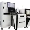
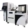
12-inch SiPh Wafer Test System
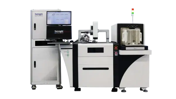
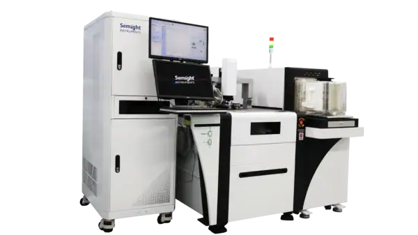
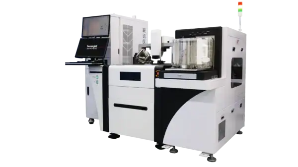
Semight sCT9002 has been fully optimized and integrated with hardware and software systems, showing significant improvements in optical alignment capability and coupling speed. The overall system adopts a modular design, with optical coupling options for fiber or fiber arrays, supporting vertical and edge coupling, and parallel testing significantly shortens testing time, effectively improving testing efficiency. The high precision and high reliability of the sCT9002 measurement results ensure the research and production of silicon photonic wafers.
Features

Automatic/Semi-automatic
Supports automatic and semi-automatic wafer loading and unloading
Compatible with 12-inch and 8-inch wafers
Wafer thickness 200μm – 2000μm

Edge Coupling
Real-time monitoring of height using nano displacement sensors to reduce the risk of damaging optical fibers
High-precision vision system, reducing errors caused by small angles

Vertical Coupling
Alignment of wafer level grating couplers using vertical coupling method
Supports spiral scanning and gradient scanning (coupling time <1.5 s)
Automated Fiber Calibration
Automated calibration script, angle calibration of the fiber array can be completed within 3mins

Modular Platform Software
Supports Notch Up/Down continuous testing, no need to reload wafer, saving testing time
Integrates most of the current silicon photonics wafer testing items cover O/O, E/E and O/E testing

Self-developed SMU
High-precision 12-channel card-type SMU, high integration, saving machine space
±10 V, 50mA, the range perfectly covers the silicon light testing requirements

Equipped with a Height Sensor
Solves the flatness variation issue of the wafer on the chuck

Test Temperature Range
Room temperature 25°~150°
(other temperatures can be customized)
Functions and Advantages
System Architecture
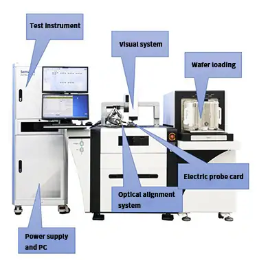
sCT9002 SiPh Wafer Test System can achieve automated wafer loading. The loaded wafers can be rotated and positioned on the stage and the testing temperature can be adjusted according to testing requirements. The active optical alignment system and electrical probes couple/connect the optoelectronic signals to the testing instruments, completing the wafer testing.
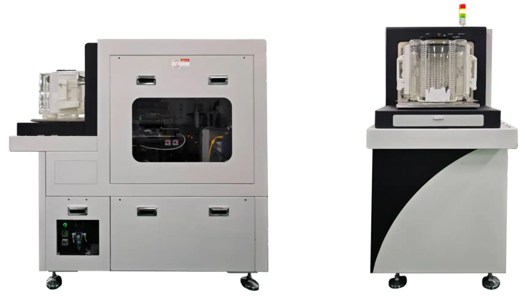
Automatic Wafer Handling
The wafer loading mode can choose between fully automatic mode or semi-automatic mode. The semi-automatic mode is suitable for laboratory verification to save investment costs; the fully automatic mode is suitable for large-scale mass production to improve production efficiency.
Specification
| CHUCK | Platform | Material | Cast iron |
| Chuck X&Y Axis | Motor type | Servo motor | |
| Travel range X*Y | ≥340 mm * 490 mm | ||
| Resolution | 0.1 μm | ||
| Positioning accuracy | ±2 μm | ||
| Max speed | 300 mm/s | ||
| Chuck Z Axis | Motor type | Stepper motor | |
| Travel range | 80 mm | ||
| Resolution | 0.2 μm | ||
| Positioning accuracy | ±2 μm | ||
| Max speed | 30 mm/s | ||
| Chuck θ Axis | Motor type | Stepper motor | |
| Travel range | ±5° | ||
| Resolution | 0.0000191° |
| Coupled Module | Motion and positioning | Hexapods + Piezo | 6 serial axis +Piezo |
| Max number of active axes | 9 | 9 | |
| Rotation for roll, yaw and pitch | Automated | Automated | |
| Stepping for X, Y, Z | Automated | Automated | |
| Rough Positioning | |||
| Travel range X,Y,Z | ±17, ±15, ±7 mm | ±15, ±15, ±10 mm | |
| Travel range θX, θY, θZ | ±9, ±8.5, ±18° | ±6, ±5, ±6° | |
| Minimum incremental motion X, Y, Z | ±0.10, ±0.10, ±0.05 μm | ±0.10, ±0.10, ±0.10 μm | |
| Minimum incremental motion θx, θy, θz | 0.05mdeg,
0.05mdeg, 0.1mdeg |
0.01deg,
0.01deg, 0.01deg |
|
| Fine Positioning | |||
| Travel range in X, Y, Z, closed loop | 80 μm | ||
| Min. incremental motion, open-loop | 0.4 nm | ||
| Min. incremental motion, closed-loop | 4 nm | ||
| Alignment Speed | |||
| Scanning time of spiraled area scan | <1.5 s | ||
| Note | For vertical coupling only, purchasing the 8-axis system is sufficient.
To be compatible with both vertical and edge coupling, the 9-axis system is required |
||
| Coupling Specification | Optical coupling speed | <1.5 s @ unilateral coupling |
| Coupling repeatability | <0.2 dB (30 times) | |
| Optical power stability | <0.2 dB @ 5 min |