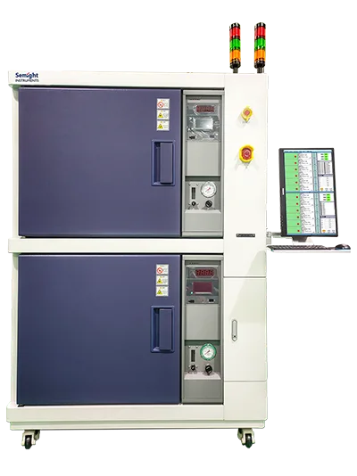
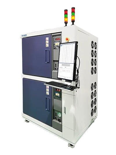
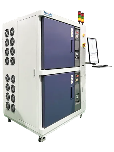
WLR0100
Wafer Level Reliability Test System
WLR0100 is a standard high-temperature reliability test system for semiconductor wafer level devices provided by Semight. It provides high-precision, high-voltage output which can store and record high-precision current for a long time, and tests related functions of devices.
- Voltage range – 0-200V software settable
- Channel hardware independent current limiting – 0-10mA software settable
- Monitoring current sampling rate – Minimum 10nA accuracy, The polling of 32 products on a single board is completed in 1 second
- Independent double temperature zone – Up to 200 ℃
- Single board support channel – 32 channels
- Channel independent gear – It can meet the accuracy and range requirements, and the channel is independent
- Product abnormal protection function – The equipment has overvoltage and overcurrent protection functions
- Support nitrogen access protection
Functions and Advantages
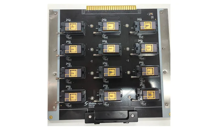
Burn-in Board for DIP Package
The supporting burn-in board adopts a gold finger structure. The following figure shows a typical DIP packaged of burn-in Board.
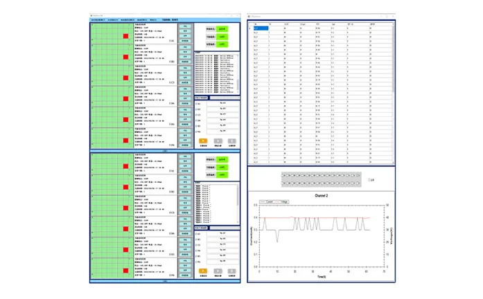
The WLR0100 test software platform is a configurable platform, including the following functions:
Support the in place pre inspection function of online products, which can detect whether the user has good plug and pull contact;
Support flexible editing and configuration of aging reliability tasks, and conduct reliability testing;
Provide intuitive data display and data analysis functions;
Support user authority control, including engineer, technician and operator.
Voltage index
| Voltage accuracy | Range | Measurement resolution | Accuracy (1 year)
± (% reading+offset) |
Typical noise (effective value)
0.1 Hz-10 Hz |
| ±200 V | 100 μV | 0.03%+10 mV | 400 μV | |
| ±40 V | 10 μV | 0.03%+2 mV | 100 μV | |
| ±20V | 10 μV | 0.03%+1 mV | 50 μV | |
| ±2 V | 1 μV | 0.03%+100 μV | 10 μV | |
| ±0.6 V | 100 nV | 0.03%+50 μV | 2 μV | |
| temperature coefficient | ±(0.15 × Accuracy index)/℃ (0℃-18℃, 28℃-50℃) | |||
| set time | <50 μs (Typical value) | |||
| overshoot | <±0.1% (Typical value, Normal, with steps ranging from 10% to 90%, full scale point, resistive load test) | |||
| Noise 10Hz-20MHz | 20V voltage source, 1A resistive load, <5 mVrms | |||
Current index
| Current accuracy | Range | Measurement resolution | Accuracy (1 year)
± (% reading+offset) |
Typical noise (effective value)
0.1 Hz-10 Hz |
| ±3 A1 | 1 μA | 0.03% + 2mA | 20 μA | |
| ±1 A | 100 nA | 0.03% + 90 μA | 4 μA | |
| ±100 mA | 10 nA | 0.03% + 9 μA | 600 nA | |
| ±10 mA | 1 nA | 0.03% + 900 nA | 60 nA | |
| ±1 mA | 100 pA | 0.03% + 90 nA | 6 nA | |
| ±100 μA | 10 pA | 0.03% + 9 nA | 700 pA | |
| ±1 μA | 100 fA | 0.03% + 200 pA | 20 pA | |
| ±10 nA2 | 10 fA | 0.06% +9 pA | 600 fA | |
| ±1 nA2 | 1 fA | 0.1% +3 pA | 60 fA | |
| ±100 pA2 | 1 fA | 0.3% +1 pA | 30 fA | |
| temperature coefficient | ±(0.15 × Accuracy index)/℃ (0℃-18℃,28℃-50℃) | |||
| set time | <100 μs (Typical value) | |||
| overshoot | <±0.1% (Typical value, Normal, with steps ranging from 10% to 90%, full scale point, resistive load test) | |||
- 3A range only supports pulse mode, with typical accuracy
- Additional specification conditions: NPLC configured with 10PLC
Pulse source indicator (4-wire)
| Minimum programmable pulse width | 100 μ S |
| Pulse width programming resolution | 1 μ S |
| Pulse width programming accuracy | ± 10 μ S |
| Pulse width jitter | 2 μ S |
| Pulse width definition | As shown in the following figure, the time from the 10% leading edge to the 90% trailing edge |
| Pulse technical indicators | Maximum current limit | Maximum pulse width | Maximum duty cycle |
| 1 | 0.1 A/200 V | DC, unlimited | 100% |
| 2 | 1 A/20 V | DC, unlimited | 100% |
| 3 | 3 A/66.6 V | 1 ms | 5% |
| 4 | 3 A/160 V | 400 μ S | 2% |
Pulse source rise time (4-wire)
| Output | Maximum output | Typical rise time1 | Typical stability time2 | Test load |
| Voltage source | 160 V | 800 μ S | 1.2 ms | Empty |
| 5 V | 40 μ S | 100 μ S | Empty | |
| Current source | 3A~100 μ A | 90 μ S | 250 μ S | With full load3 |
| 1 μ A | 300 μ S | 600 μ S | With full load3 | |
| 10 nA | 5 ms | 10 ms | With full load3 | |
| 1 nA | 10 ms | 50 ms | With full load3 | |
| 100 pA | 100 ms | 500 ms | With full load3 |
- The time required for the pulse front to travel from 10% to 90%
- The time required for the pulse to reach 1% of the final value
- Test conditions: Normal pure resistance full load voltage rises to 6V
Output establishment time
| Output | Range | Typical output establishment time1 | Test conditions | ||
| Fast2 | Normal | Slow | |||
| Voltage source | 200 V | <five hundred μ S | <nine hundred μ S | <2 ms | The time required to reach within 0.1% of the final value under open circuit load conditions. Stepping is within the range of 10% to 90% |
| 40 V | <two hundred μ S | <four hundred μ S | <nine hundred μ S | ||
| 20 V | <sixty μ S | <one hundred μ S | <five hundred μ S | ||
| 2 V | <fifty μ S | <fifty μ S | <fifty μ S | ||
| Current source | 3 A~100 μ A | <fifty μ S | <one hundred μ S | <0.8 ms | Under normal conditions and full load, the voltage output reaches 6V. Reaching within 0.1% of the final value (for 3 A The time required for a range of 0.3%. Step is 10% of the range to 90% |
| 1 μ A | <three hundred μ S | <four hundred μ S | <1 ms | ||
| 10 nA | <10 ms | <10 ms | <10 ms | ||
| 1 nA | <50 ms | <50 ms | <50 ms | ||
| 100 pA | <500 ms | <500 ms | <500 ms | ||
- Output conversion rate: Fast, Normal, Slow. Users can adjust APFC parameters based on load characteristics to obtain appropriate setup time or stability
- Fast mode may produce significant overshoot under different range or load conditions. It is recommended to use normal or slow mode for overshoot sensitive devices
